-
Contract Manufacturing of Glass Substrate Sensors (Foundry/OEM/ODM)


We bring your business ideas to life with Japan Display’s cutting-edge glass substrate microfabrication technology and manufacturing capabilities.


TFT Microfabrication Expertise from Display Technology × Glass Substrates
JDI leverages its TFT microfabrication technology, cultivated through display manufacturing, to sensor production. Utilizing high-precision processes and large 730 mm ×920 mm glass substrates, we offer foundry services ideal for large-area, high-performance sensors.
One-Stop Foundry Service
From process development to mass production and inspection, we offer fully integrated support. We propose optimized designs and build customized processes tailored to each customer’s specifications, enabling smooth ramp‑up and commercialization while reducing mask costs and lead times.

Proven Track Record and High-Quality Control for Various Sensors
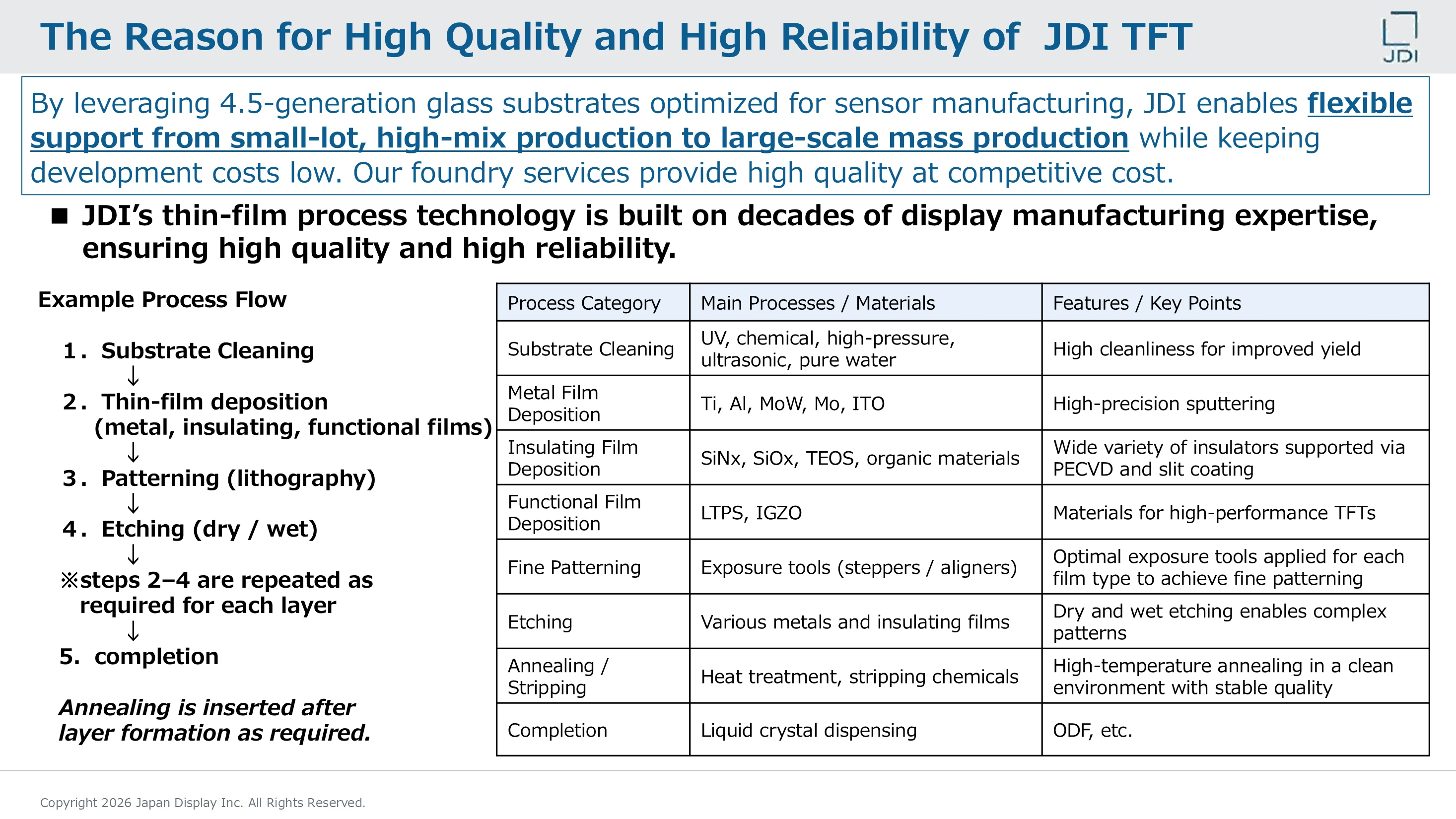
We have extensive experience in contract manufacturing of various sensors, including X-ray sensors, IR sensors, and fingerprint sensors, tailored to diverse applications. Through rigorous cleaning, film deposition, photolithography, and inspection processes, we ensure superior reliability and high yield. “Quality honed through display manufacturing” — JDI enhances manufacturing precision in sensor foundry services.
Advanced TFTs Integrated on Glass Substrates
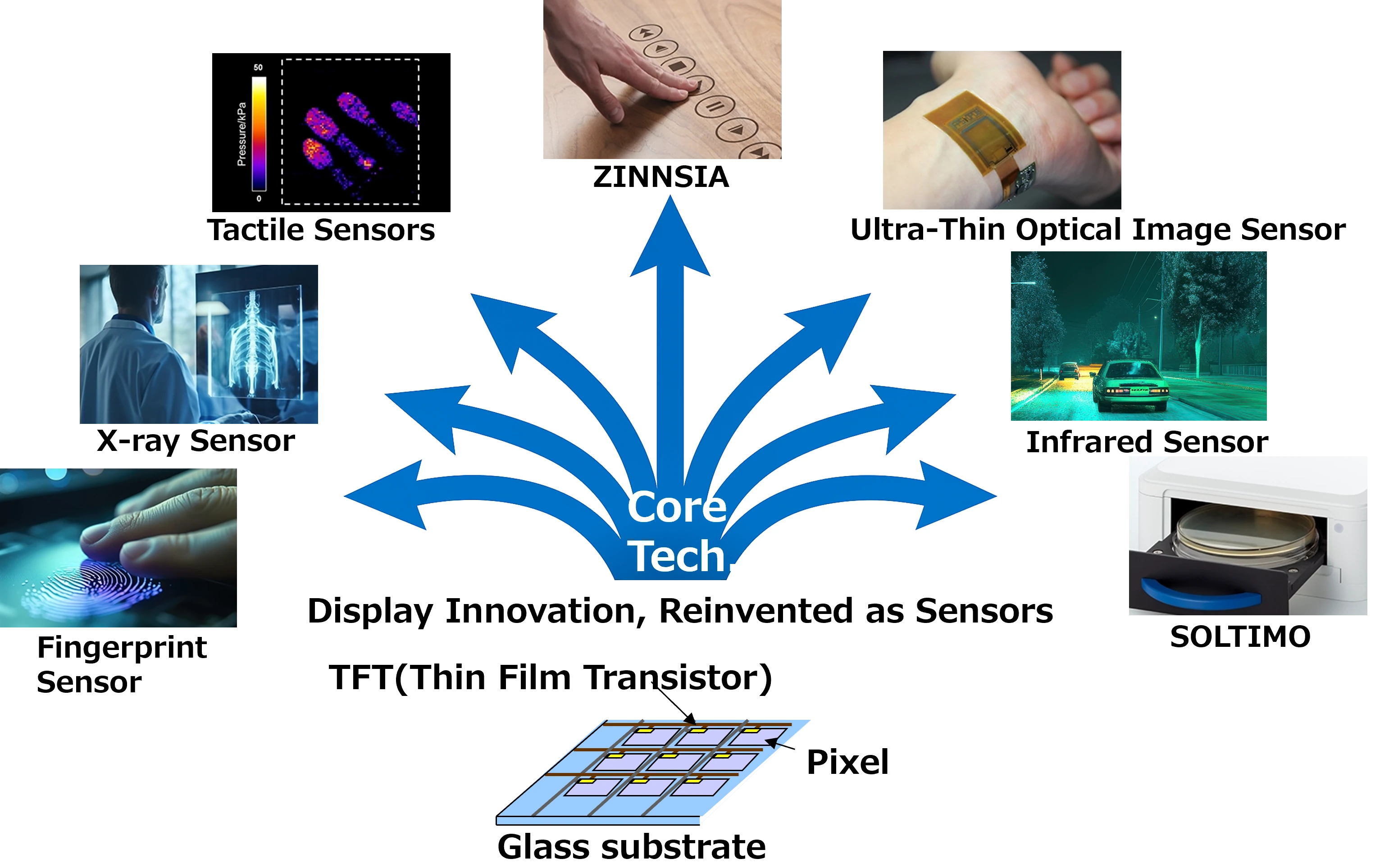
Japan Display (JDI) has spent many years advancing thin‑film transistor (TFT) technology, continually pushing the limits of microfabrication.Our proprietary equipment, known for its outstanding reliability, combined with our refined technical expertise, enables the creation of innovative devices.Leveraging these strengths, we provide foundry services focused on glass‑substrate sensor manufacturing, as well as OEM and ODM production, to deliver new value to our partners.
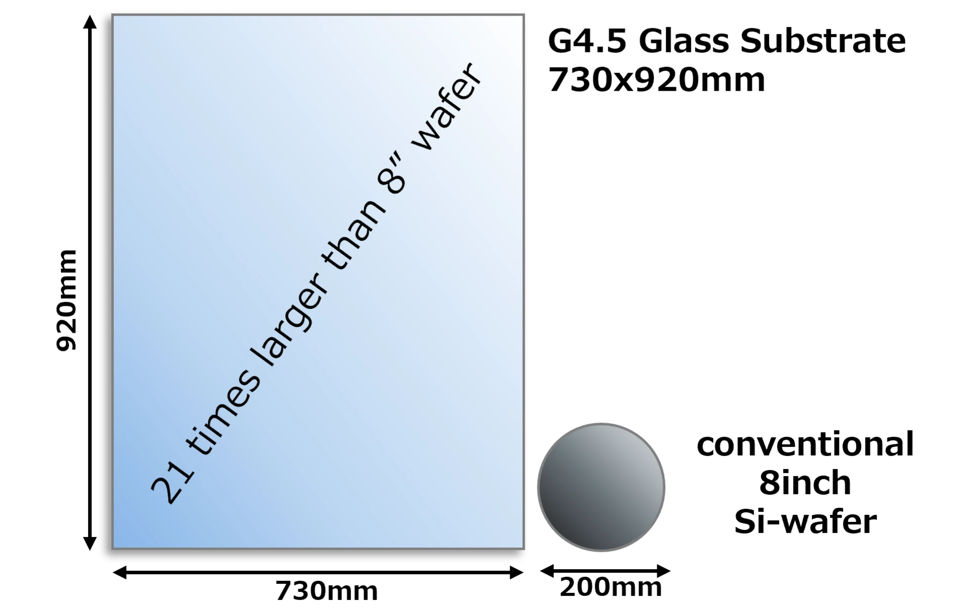
JDI’s 4.5-generation glass substrates offer a processing area approximately 21 times larger than an 8-inch silicon wafer, well-suited for large-area sensor manufacturing.With expanded design freedom and high productivity, we bring new possibilities to future device development.
Ishikawa Fab
Introduction of Our Main Factory:Ishikawa Fab
- 4.5‑Generation Glass Substrate Production
- Certified to ISO 9001, ISO 14001, and IATF 16949
- Extensive mass‑production experience ranging from early mobile devices to
high‑resolution VR and automotive applications
- PIN deposition CVD equipment in operation for 4.5‑generation glass substrates
- 30 minutes by taxi from Komatsu Airport
-Get off at "Matto" station of JR Hokuriku line : 20min.
drive by taxi till JDI Ishikawa Fab
Example of Our Standard Engagement Process
Available Process
The linked documents are the property of Japan Display, and its usage is in accordance with the terms and conditions of our website.
Download Our Available Process from the following link.
Application Example
Capacitive Touch Sensors
Large-area sensors enabled by G4.5 glass substrates
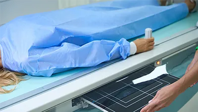
X-ray Sensors

High-resolution X-ray imaging using PIN photodiodes combined with TFTs
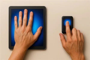
Tactile Sensors
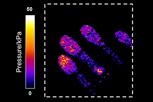
Application example combining advanced TFT technology with pressure-sensitive sheets
Logic Circuits
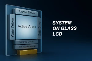
LTPS logic and driver circuits integrated on glass Logic and arithmetic circuits can be integrated directly on glass substrates
For inquiries about Contract Manufacturing of Glass Substrate Sensors (Foundry/OEM/ODM),
please contact us.


Global No. 1Technology Leadership to Best Serve Customers and Deliver PersonalTech For A Better World