-
Conformable Thin Image Sensor


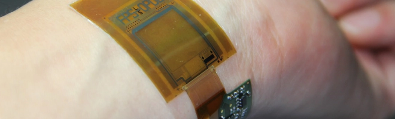
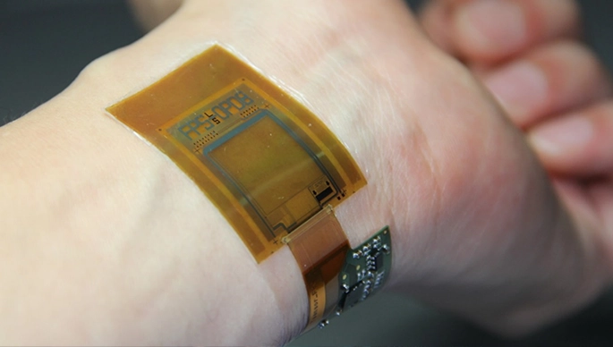
The Conformable Thin Image Sensor is a thin sensor that forms a light sensor layer on a flexible sheet substrate for displays. The thin and flexible design minimizes wearing stress and makes it possible to be worn on a daily basis.
A thin-film transistor circuit can be formed on the sheet substrate to read the signal from the light sensor layer as an image.
The light sensor layer is an organic material sensitive to near-infrared light, so it can measure subcutaneous vein images and pulse waves.
Since it can constantly measure biometric signals such as pulse waves while identifying individuals based on their vein images, it can construct a highly secure measurement system.
Capable of Simultaneous Measurement of Fingerprints, Veins, and Pulse Waves
By integrating high-mobility low-temperature polysilicon (LTPS) thin-film transistors and high-sensitivity organic light detectors, we have made it possible to measure biometric information that requires high-resolution imaging, such as fingerprints and veins used for biometric authentication, and the distribution of pulse waves that require high-speed reading, with a single image sensor.
Enhanced Security Strength
By simultaneously acquiring biometric information (fingerprints, veins) and biometric signals (pulse waves), it is possible to prevent imitation and impersonation, making it suitable for application to authentication systems with high security.
Lightweight and bendable.
The image sensor can be formed to a thickness of 15 micrometers.
Application Example
Sample specifications
| Specifications 1 | Specifications 2 | |
|---|---|---|
| Sensor Area | 12.6×12.8mm2 | 29.6×39.5mm2 |
| Resolution | 252×256 | 126×168 |
| Precision | 508dpi | 108dpi |
| Reading Speed | Up to 41Hz | Up to 270Hz |
dpi: Number of sensors per inch
Reference
T. Yokota et al., “A conformable imager for biometric authentication and vital sign measurement,” Nature Electronics, DOI: 10.1038/s41928-019-0354-7, 2020.
For enquiries about Conformable Thin Image Sensors, please contact us.


Global No. 1Technology Leadership to Best Serve Customers and Deliver PersonalTech For A Better World